- 您现在的位置:买卖IC网 > Sheet目录1992 > CY284108ZXC (Silicon Laboratories Inc)IC CLOCK SERV CK410B 56TSSOP
CY284108
...................... Document #: 38-07713 Rev. *B Page 10 of 16
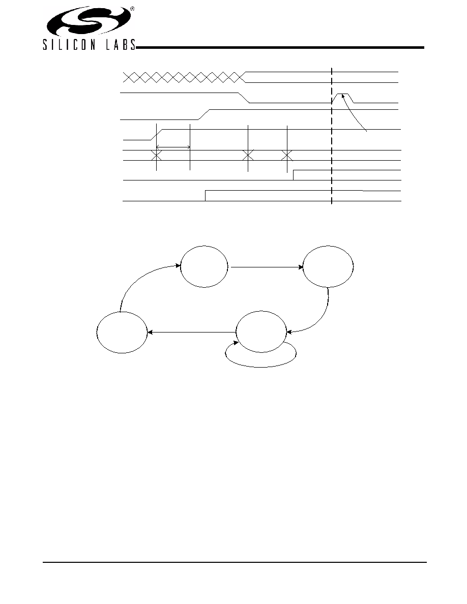
FS_A, FS_B,FS_C
VTT_PWRGD#
PWRGD_VRM
VDD Clock Gen
Clock State
Clock Outputs
Clock VCO
0.2-0.3 ms
Delay
State 0
State 2
State 3
Wait for
VTT_PWRGD#
Sample Sels
Off
On
State 1
Device is not affected,
VTT_PWRGD# is ignored
Figure 6. VTT_PWRGD# Timing Diagram
VTT_PWRGD# = Low
Delay >
0.25 ms
S1
Power Off
S0
VDD_A = 2.0V
Sample
Inputs straps
S2
Normal
Operation
Wait for <1.8 ms
Enable Outputs
S3
VTT_PWRGD# = toggle
VDD_A = off
Figure 7. Clock Generator Power-up/Run State Diagram
发布紧急采购,3分钟左右您将得到回复。
相关PDF资料
CY28410OXC-2
IC CLOCK CK410 GRANTSDALE 56SSOP
CY28410OXC
IC CLOCK CK410 GRANTSDALE 56SSOP
CY28411ZXC
IC CLOCK CK410M ALVISO 56TSSOP
CY28442ZXC-2
IC CLOCK ALVISO PENTM 56TSSOP
CY28445LFXC-5
IC CLOCK CALISTOGA CK410M 68QFN
CY28446LFXC
IC CLOCK CALISTOGA CK410M 64QFN
CY28447LFXC
IC CLOCK CALISTOGA CK410M 72QFN
CY28547LFXCT
IC CLOCK CK505/410M INTEL 72QFN
相关代理商/技术参数
CY284108ZXCT
功能描述:时钟发生器及支持产品 Server, CK410B RoHS:否 制造商:Silicon Labs 类型:Clock Generators 最大输入频率:14.318 MHz 最大输出频率:166 MHz 输出端数量:16 占空比 - 最大:55 % 工作电源电压:3.3 V 工作电源电流:1 mA 最大工作温度:+ 85 C 安装风格:SMD/SMT 封装 / 箱体:QFN-56
CY28410OC
制造商:SPECTRALINEAR 制造商全称:SPECTRALINEAR 功能描述:Clock Generator for Intel Grantsdale Chipset
CY28410OCT
制造商:SPECTRALINEAR 制造商全称:SPECTRALINEAR 功能描述:Clock Generator for Intel Grantsdale Chipset
CY28410OXC
功能描述:时钟发生器及支持产品 SysClk Intel Lakeprt & Grantsdale Chipset RoHS:否 制造商:Silicon Labs 类型:Clock Generators 最大输入频率:14.318 MHz 最大输出频率:166 MHz 输出端数量:16 占空比 - 最大:55 % 工作电源电压:3.3 V 工作电源电流:1 mA 最大工作温度:+ 85 C 安装风格:SMD/SMT 封装 / 箱体:QFN-56
CY28410OXC-2
功能描述:时钟发生器及支持产品 SysClk Intel Lakeprt & Grantsdale Chipset RoHS:否 制造商:Silicon Labs 类型:Clock Generators 最大输入频率:14.318 MHz 最大输出频率:166 MHz 输出端数量:16 占空比 - 最大:55 % 工作电源电压:3.3 V 工作电源电流:1 mA 最大工作温度:+ 85 C 安装风格:SMD/SMT 封装 / 箱体:QFN-56
CY28410OXC-2T
功能描述:时钟发生器及支持产品 SysClk Intel Lakeprt & Grantsdale Chipset RoHS:否 制造商:Silicon Labs 类型:Clock Generators 最大输入频率:14.318 MHz 最大输出频率:166 MHz 输出端数量:16 占空比 - 最大:55 % 工作电源电压:3.3 V 工作电源电流:1 mA 最大工作温度:+ 85 C 安装风格:SMD/SMT 封装 / 箱体:QFN-56
CY28410OXCT
功能描述:时钟发生器及支持产品 SysClk Intel Lakeprt & Grantsdale Chipset RoHS:否 制造商:Silicon Labs 类型:Clock Generators 最大输入频率:14.318 MHz 最大输出频率:166 MHz 输出端数量:16 占空比 - 最大:55 % 工作电源电压:3.3 V 工作电源电流:1 mA 最大工作温度:+ 85 C 安装风格:SMD/SMT 封装 / 箱体:QFN-56
CY28410ZC
制造商:SPECTRALINEAR 制造商全称:SPECTRALINEAR 功能描述:Clock Generator for Intel Grantsdale Chipset